


Transistoren
We look at the tiny devices that have reshaped the world of electronics.
Along with the solid-state diode, the point-contact transistor--invented in 1947 at Bell Labs--started the semiconductor revolution and has gone on the become one of the rudimentary devices in today's electronic equipment. The transistor, whether in discrete or IC form, is at the heart of most modern circuitry. Therefore, understanding how transistors function will help you properly design circuits containing them, and in case of a failure, enable you to find and correct the problem.
Bipolar-Transistor Composition:
A bipolar transistor is
basically a two PN junctions connected back-to-back within the same
piece of semiconductor material and sharing a common P- or N-doped
semiconductor region. There are two types of bipolar transistor, the NPN
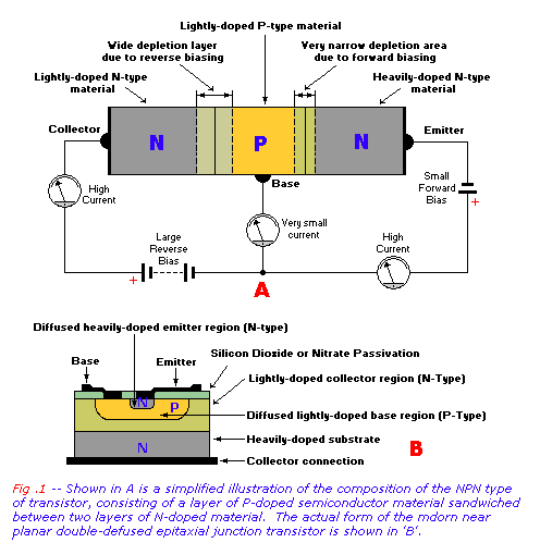
and the PNP. Fig. 1A is a simplified illustration of the composition of
the NPN type of transistor. In our illustration, the NPN type unit is
shown as P-doped semiconductor material sandwiched between two layers of
N-doped material. The composition of a PNP transistor is just the
opposite of that, (i.e. the N- and P-doped materials in the transistor
are interchanged). It follows then that biasing considerations for NPN
units are also opposite from those for the PNP unit.
Note from Fig. 1A that a bipolar transistor is comprised of a center
region called the base surrounded by two other regions known as the
collector and the emitter. The difference between them will be discussed
shortly. The two junctions are arranged so that they are very close
together; that's done by making the shared base region very thin and
lightly doped. That causes the two junctions to interact with one
another. Conduction is the collector-base junction depends largely on
what happens in the emitter-base junction.
Because the region is
lightly doped, it has a relatively small number of free carriers (holes
in a P-type base and electronics in an N-type base) to conduct current.
On the other hand, the emitter region is quite heavily doped, containing
a much larger amount of donor impurity (for the NPN type) or acceptor
impurity (for the PNP type), so there are many more free carriers
available in the emitter region to conduct current than in the adjacent
base region. Because of that, the emitter-base junction, when forward
biased, conducts much the same as a common PN junction diode.
The
current that flows (composed of electrons for NPN units and holes, in
the case of PNP transistors) is mainly from the emitter to the base
rather than vice versa. That is where the emitter derives its name--it
emits or injects current carriers in the other regions of the device.
The third region of a transistor, the collector, is lightly doped, much the same as the base, except with the opposite type of doping impurity, so it (like the base region) has relatively few free carriers available to conduct current in the normal way. The collector-base junction is normally reverse biased, so a depletion layer forms, spreading out on either side of the junction. The depletion layer effectively removes the carriers that would otherwise balance out the charges on the fixed impurity atoms of the crystals, setting up a potential barrier to match the applied reverse voltage.
To the normal majority carriers in the base and emitter, that potential
barrier is a big wall that must be overcome before they can pass to the
other side. So just as in the case of a normal diode, virtually no
current flows across the collector-base junction when left to its own
devices. However, the junction is not left to its own devices.
Remember that the base region is deliberately made very thin and lightly
doped, while the emitter is made much more heavily doped. Because of
that, applying a forward bias to the emitter-base junction causes vast
majority carriers to be injected into th the base, and straight into the
reverse-biased collector-base junction. Those carriers are actually
minority carriers in the base region, because that region is of opposite
semiconductor type to the emitter. To those majority-turned-minority
carriers, the collector-base junction depletion region is not a barrier
at all but an inviting, accelerating filed; so as soon as they reach the
depletion layer, they are immediately swept into the collector region.
That effect is illustrated in Fig. 1A, which (hopefully) will help you to understand what is going on. The diagram shows a NPN transistor, but the action in a PNP unit is similar except for the opposite region polarity and conduction mainly by holes rather than electrons.
From a practical point of view, the behavior of bipolar transistors means that, unlike the simple PN-junction diode, it is capable of amplification. In effect, a small input current made to flow between the emitter and collector. Only a small voltage--around 0.6 volts for a typical silicon transistor--is needed to produce the small input current required.
In contrast, the reverse-bias voltage applied across the collector-base junction can be much larger; typically anywhere from 6 to 90 volts or more. So in producing and being able to control a larger current in this much higher-output circuit, the transistor's small input current and voltage can achieve considerable voltage, power, and current, gains.
Bipolar transistors, therefore, work very well as both amplifiers and electronics switches. That is why they have become the workhorses of modern electronics, virtually replacing the vacuum tube. The diagram in Fig. 1A is designed to show how a bipolar transistor works, rather than its physical construction. The actual form of the modern, planar, double-defuse epitaxial-junction transistor is shown in Fig. 1A.
The collector region is formed from a lightly doped layer grown epitaxially on the main substrate, which is made from the same type (but more heavily doped) material to provide a low resistance connection. Here, both are N-doped material; for a PNP transistor, they would be P-doped material.
The base region is formed by lightly diffusing the opposite type impurity into a medium-sized area of the chip surface to reverse that type of area and create the base-collector unction. The emitter region is formed by a second and heavier diffusion over the smaller area inside the first, but this time with the same kind of impurity as used for the epitaxial collector region.
The second diffusion is very carefully controlled so that the emitter region that results extends almost--but not quite--to the bottom of the base. That leaves the area of the base right below the emitter quite thin to ensure that as many as possible of the carriers are injected from the emitter region will be swept through to the collector. The thinner that active base region, the higher (in general) the gain of the transistor.
Note that although the collector and emitter regions are made of the same type of semiconductor material, the two are physically quite different. The emitter is heavily doped (for a good carrier injection) and can be relatively small since the emitter-base junction does not need to dissipate much power (heat). In contrast, the collector is lightly doped (for a wide depletion area) and its junction is much larger since, being reversed biased, it must dissipate much more power.
Connections to the emitter and base regions are made by way of aluminum electrodes deposited on the surface. Thin wires are bonded to the electrodes for connection to the main device leads. The low-resistance substrate itself is used to connect to the collector region.
That is the basic construction used for most modern bipolar transistors, whether they are discrete units or part of an

IC containing thousands of transistors. The main difference is size, although, in an IC, the collector region of the transistor will generally be in an epitaxial layer grown on the opposite kind of substrate, and separated by diffused walls (of the opposite type material) to separate the transistors from each other.
In an IC, the active part of an individual transistor might only be a couple micrometers square, while a very large transistor (used to switch hundreds of amperes) might be on a single wafer of 10 mm or more in diameter. Typical small-to-medium power, discrete transistors used in consumer and hobby electronics are grown on chips measuring from 1- to about 3-mm square--the rest of the component is protective packaging.
Transistor Operation:
Refer to Fig. 2, a PNP version of the
illustration shown in Fig. 1A. Note that both are essentially the same,
except that in this instance, the collector is more negative than the
base or the emitter. That is an important characteristic to remember
when it comes to the operation of bipolar transistors.
If a positive voltage is applied to the P-doped emitter (to the left),
current will be swept through the base-emitter junction--with the holes
from the P-doped material moving to the right and the electrons form the
N-doped material moving to the left. Some of the holes moving into the
N-doped base region will combine with the electrons and become
neutralized, while others will migrate to the base-collector junction.
Normally, if the base-collector junction is negatively biased, there
would be no current flow in the circuit. However, there would be
additional holes in the junction to travel to the base-collector
junction, and electrons can then travel toward the base-emitter
junction, so a current flows even through that section of the sandwich
is biased (at cutoff) to prevent conduction. Most of the current travels
between the emitter and collector and does not flow out through the
base.
The amplitude of the collector current depends principally on
the magnitude of emitter current (e.g., the collector current). Note
that between each PN junction, there is an area known as the depletion
or transition region that is similar in some characteristics to a
dielectric layer. That layer varies in accordance with the operating
voltage. The semiconductor materials on either side of the depletion
regions constitute the plates of a capacitor. The base-collector
capacitance is indicated in Fig. 2 as Cbc, and the
base-emitter capacitance is designated Cbe. A change in
signal and operating voltages causes a non-linear change in those
junction capacitances.
There is also a base-emitter resistance (Rbe that must be
considered. In practical transistors, emitter resistance is on the order
of a few ohms, while the collector resistance is many hundreds or even
thousands of times larger. The junction capacitance in combination with
the base-emitter resistance determine the useful upper-frequency limit
of a transistor by establishing an RC time constant.
Because the
collector is reversed biased, the collector-to-base resistance is high.
On the other hand, the emitter and collector currents are substantially
equal, so the power in the collector circuit is larger than the power in
the emitter circuit.
(P = I2R, so the powers are
proportional to the respective resistances, if the currents are the
same.)
In practical transistors, emitter resistance is on the order of a few
ohms, while the collector resistance is many hundreds or thousands of
times larger, so power gains of 20 to 40dB, or even more, are possible.
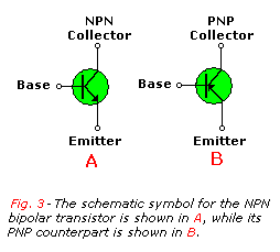 Figure 3 shows the
schematic symbols for both the NPN and PNP version of the bipolar
transistor. The first two letters of the designators (NPN or PNP)
indicate the polarities of the voltages applied to the collector and
emitter in normal operation. For example, in a PNP unit, the emitter is
made more positive with respect to the collector and the base, and the
collector is made more negative with respect to the base. Another way of
saying that is: the collector is more negative than the base and the
base is more negative than the emitter.
Figure 3 shows the
schematic symbols for both the NPN and PNP version of the bipolar
transistor. The first two letters of the designators (NPN or PNP)
indicate the polarities of the voltages applied to the collector and
emitter in normal operation. For example, in a PNP unit, the emitter is
made more positive with respect to the collector and the base, and the
collector is made more negative with respect to the base. Another way of
saying that is: the collector is more negative than the base and the
base is more negative than the emitter.
Transistor Amplifiers:
Transistors are among the most
commonly used building blocks in electronics. While they can be used as
electronically controlled switches, they are widely configured for
amplifier use. In fact, the vast majority of electronic circuits contain
one or more amplifiers of some type or another.
However, what
exactly do we mean by the term amplifier? By definition an amplifier is
a circuit that draws power from a source other than the input signal and
produces an output that is usually an enlarged reproduction of the input
signal.

We say usually because not all amplifiers are used to magnify the input
signal--buffer amplifiers (often called unity-gain amplifiers) are not
designed to magnify the input signal. When operated as a buffer, the
transistor is used to isolate one stage from the effects of one that
follows. Since buffer amplifiers provide no increase in signal level, a
10-millivolt (mV) signal applied to the input of a unity-gain amplifier
produces an output signal at the same 10-mV level (a carbon copy of the
input signal).
There are may types of amplifiers, however, and all
fall into one of two broad categories: voltage amplifiers or current
(often referred to as a power) amplifiers. The term voltage amplifier
implies to a circuit in which a low voltage is applied to the input to
produce a higher voltage at the output. The term power amplifier is
generally reserved for those that supply an appreciable power (or
current) increase to the load.
Because a vast array of amplifier
circuits in use in modern electronics, amplifier circuits are often
subdivided by application--AF, IF, RF, Instrumentation, op-amp, etc.
Another way of categorizing amplifiers is by configuration:
common-emitter, common-collector, and common-base for example. The
important parameters in such circuits are the cutoff frequency and the
input/output impedances. The cut-off frequency at which the gain of an
amplifier falls below 0.707 times the maximum gain of the circuit. The
input impedance is the output impedance of the transistor.
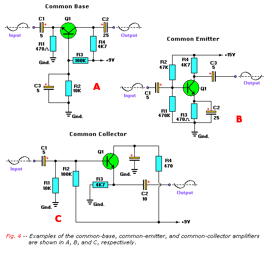
An example of a common-base amplifier is shown in Fig. 4A. The optimum load impedance can range from a few thousand ohm to 100,000 ohms, depending on the circuit's requirements. In this type of circuit, the output signal (at the collector) is in phase with the input signal (applied at the emitter). THe current that flows through the base resistance of the transistor is therefore in phase as well, so the circuit tends to be regenerative and will oscillate if the current-amplification factor is greater than one.
A common-emitter (also called a 'grounded-emitter') amplifier is shown in Fig. 4B. Base current in this amplifier configuration small and the input impedance is therefore fairly high (several thousand ohms on the average). Collector resistance on the other hand, can be tens of thousands of ohms, depending on the signal's source impedance. The common-emitter amplifier has a lower cutoff frequency than does the common-base type, but gives the highest power gain of the three configurations. Note that the output signal is 180° out-of-phase with (or the opposite of) the input (base-current) signal, so the feedback that flows through the small emitter resistance is negative (degenerative), keeping the circuit stable. The common-emitter amplifier is one of the most often seen configurations for the bipolar transistor.
The common-collector amplifier (also referred to as an emitter follower), see Fig. 4C, has a high input impedance and a low output impedance.
The impedance is approximately: 
The fact that the input resistance is directly related to the load resistance is a disadvantage of this type of amplifier if the load is one whose resistance or impedance varies with frequency.
The current transfer ratio of this type of circuit is: 
and the cutoff frequency is the same as in the common-emitter amplifier circuit. The output and input currents of this type of circuit are in phase.
 Amplifier Classifications:
Amplifiers may be otherwise classified by their specific operational
characteristics, in particular, the bias voltages between the
emitter-base and base-collector junctions. The relationship between the
bias voltage and the cutoff voltage of an amplifier is what classifies
an amplifier as being class A, B, C, or AB. Each class has a specific
characteristic that makes it most suitable for a particular application.
In a class-A amplifier--which is the least efficient, but offers the
least distortion--the transistor is biased so that its quiescent
operation point is in the middle of the power-supply extremes, i.e., the
transistor is always turned on and the resulting output varies around
the bias voltage; see the output waveform in Fig. 5A. Because of that,
the input signal must be small enough so that its positive and negative
swings do not drive the amplifier near the non-linear cutoff and
saturation regions.
Since a high-value resistor is used to change
the output voltage to a current (I = V/R) in a class-A
configuration, the output current is small. That is important since
current flows at all times in such amplifiers, with or without an input
signal. Power is wasted and efficiency (the ratio of output to total
power consumed) is low--only about 20-25%--in call-A amplifiers. Class-A
amplifiers can be configured for single-ended or push-pull operation and
are used in AF (audio frequency), IF (intermediate frequency), and RF
(radio frequency) applications.
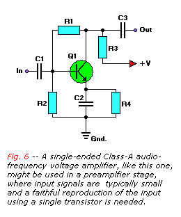 Class-A operation is suitable for voltage
amplifiers. In a voltage amplifier, the emphasis is on the magnitude of
the output voltage. Figure 6 shows a single-ended class-A amplifier.
Such an amplifier might be used in a preamplifier stage, where input
signals are typically small, and a faithful reproduction of the input
using a single transistor is needed. That configuration allows a small
input current to control current drawn from a power source, and thus
produce a stronger replica of a weaker original signal.
Class-A operation is suitable for voltage
amplifiers. In a voltage amplifier, the emphasis is on the magnitude of
the output voltage. Figure 6 shows a single-ended class-A amplifier.
Such an amplifier might be used in a preamplifier stage, where input
signals are typically small, and a faithful reproduction of the input
using a single transistor is needed. That configuration allows a small
input current to control current drawn from a power source, and thus
produce a stronger replica of a weaker original signal.
In Class-B operation, the transistor is biased at cutoff (see Fig. 5B), so that output current flows during only half of the input cycle. It is used where high efficiency and low distortion are required--for instance, in power-output configurations. When the Class-B amplifier is used for audio applications, two such amplifiers connected in the push-pull configuration are required, so that current can flow alternately through the two amplifiers. In other words, on amplifier is turned on, while the other is turned off.
On the other hand, when the Class-B amplifier is used in RF
applications, it can be configured for single-ended operation. Since, in
the absence of an input signal its current output is negligible, it is
used where high efficiency (60-70%) and low distortion are required,
which is very important in high-power amplifiers.
Class-AB
amplifiers (see Fig. 5C) are biased somewhere between Class-A and
Class-B operation, and have efficiencies (25-35%) and distortion
characteristics that lie between those of Class-A and Class-B
amplifiers. Class-AB amplifiers require a somewhat larger input signal
than do Class-A amplifiers. The class-AB amplifier is used in push-pull
configurations for both audio-and radio-frequency applications.
In Class-C operation--which has the highest efficiency (perhaps more than 90%), but offers the greatest distortion--the transistor is biased beyond the cutoff region (see Fig. 5D). Because of that, output output current flows during less than half (about a third) of the input cycle, making it unsuitable for amplifying signals of varying amplitude, such as audio. That type of amplifier is normally used to amplify a signal of fixed amplitude; for instance, it is often used in RF power output stages of a transmitter. Current in a Class-C amplifier flows in a series of power pulses that excite an LC-tank circuit into oscillation. Because of that the output waveform is a sinewave, that varies in amplitude if modulated. Class-C amplifiers can be configured for push-pull or single-ended operation. Table 1 summarizes the conduction angles and efficiency ratings of the various classes of transistor amplifier.
color = '#ff0000' size = '4'>'The bipolar junction transistor is still one of the cornerstone's of modern solid-state electronics. Learn (or review) the basics of this important active device.
The Bipolar Junction Transistor (BJT) triggered the revolution in modern
solid-state electronics in the 1960's. Although the discrete
small-signal BJT has since yielded to the integrated circuit (IC) in
economic importance, it lives on in the form of discrete linear and
switching power transistors as well as radio-frequency transistors into
the microwave region.
The principles behind the operation of the
BJT are important to the understanding of many of today's most popular
linear and digital integrated circuits. Moreover, the transistor
families--TTL, Schottky TTL, and emitter-couple logic (ECL) are BJT's.
This article focuses small-signal BJT's and practical circuits that can
be made with them. They function either as linear amplifiers or digital
switches.
The term bipolar junction transistor (BJT) distinguishes
it from the junction field-effect transistor or JFET.
 BJT
Basics:
BJT
Basics:
A BJT is a three-terminal (base, emitter, and
collector) device. There are two types: NPN and PNP. Today both are
typically made by the double-diffusion process that involves the
deposition of two additional layers of doped silicon on a doped silicon
wafer.
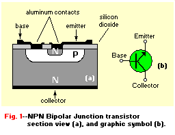
Figure 1-a shows the cross section of an NPN BJT. Its base
and emitter terminals are metal depositions on top of the silicon wafer,
and its collector is the metalized lower surface of the wafer. Figure
2-a shows the cross section of a PNP BJT. It is similar to the NPN BJT,
except that the N- and P-type materials have changed places.
Figure
1-b and 2-b are the schematic symbols for the NPN and PNP transistors,
respectively. Notice that they are the same except for the direction of
the arrowhead within the symbol at the emitter terminal. This difference
will be explained shortly.
The term bipolar means that the BJT's
operation depends on the movement of two different carriers: electrons
and holes. In NPN BJT's the electron is the majority carrier and the
hole is the minority carrier. This situation is reversed in the PNP BJT.
By contrast, all filed-effect transistors (JFET's and MOSFET's) depend
upon the movement of only one carrier, either electrons or hoes,
depending on whether they are N-channel or P-channel devices, so they
are technically unipolar devices. (For more on this, see Electronics
Now, April and May 1993).
The voltage on the collector of the
NPN BJT must be positive with respect to its emitter if current Ic
is to flow. That current will increase with a positive bias on the base.
Figure 3-a shows how a small input current applied at the base (Ib)
of the NPN BJT can control Ic. The arrowhead indicates the
direction of conventional current flow--collector to emitter. Note that
it is in the same direction as the arrowhead in the symbol for the NPN
transistor. (Electrons flow in the direction opposing the arrowhead.)
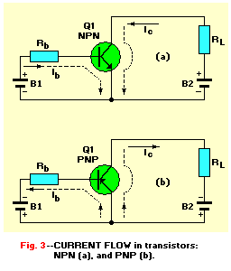
Similarly, the PNP transistor requires a negative
collector supply with respect to its emitter to operate, and a negative
base bias to increase conduction. Fig. 3-b shows conventional current
flow in the PNP BJT from the emitter to the collector, as shown in the
symbol for the NPN transistor, but opposite to that shown in Figure 3-a.
Most of the common commodity NPN and PNP BJT's available from
electronics distributors and retail stores have been standardized and
are made by many different suppliers around the world. Table 1 lists the
basic characteristics of two typical general-purpose, small-signal BJT's
that are included in the projects discussed in this article: the 2N3904
NPN-type and the 2N3906 PNP-type. Both are packaged in small, three-pin
plastic cylindrical TO-92 packages with flat faces.
Brief definitions for the parameters in Table 1 are:
Power
dissipation is the maximum mean power that the BJT can dissipate without
an external heatsink, at normal room temperature, 25°C.
FT
is the gain-bandwidth product, the frequency at which the common-emitter
forward current gain is unity.
VCBO is collect-base
voltage (emitter open), the maximum voltage that can be impressed across
collect and emitter when the base is open.
VCEO is the
collector-emitter voltage (base open), the maximum voltage that can be
impressed across collector and emitter when the base is open.
 IC(max) is the maximum mean
current that should be allowed to flow through the collector terminal of
the BJT.
IC(max) is the maximum mean
current that should be allowed to flow through the collector terminal of
the BJT.
hFE is the DC forward-current gain, the ratio
of DC collector current to DC base current for a transistor in a
common-emitter configuration.
The gain-bandwidth product, the frequency at which common emitter forward current gain is unity, applies in the following way: if a transistor in a voltage feedback circuit has a voltage gain of X 100, its bandwidth will be one hundredth of gain bandwidth value. However if the voltage gain is reduced to X 10, the bandwidth will increase to that value divided by 10.
Transistor Characteristics:
A knowledge of the static and
dynamic characteristics of BJT's will be useful in obtaining the optimum
performance from the device. Static characteristics are values obtained
when the device is in a test circuit and operated under DC conditions
with the measurements made by an ohmmeter.
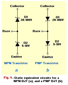
Figure 4-a shows the
static equivalent circuit of an NPN BJT, and Figure 3-b shows the static
equivalent of a PNP BJT. Each device can be considered as equivalent to
a pair of reverse-biased zener diodes in series between the collector
and emitter terminals, with the base terminal connected to the common
point between to the two zeners.
Examination of Figs. 1-a and 2-a
shows that each BJT is really two diodes: the emitter and base form one
PN diode with an emitter-base junction, and the base and collector form
a second PN diode with a base-collector junction. When these diodes are
properly biased, they reach an avalanche or zener breakdown point.
In most small-signal BJT's, the base-to-emitter junction has a typical
zener value of 5 to 10 volts, while the base-to-collector junction has a
typical zener value of 20 to 100 volts. Thus, if the base-to-emitter
junction of the BJT is forward biased, it exhibits the characteristics
of a zener diode. The forward-biased junction in a silicon BJT blocks
virtually all current until the bias voltage rises to about 600
millivolts.
 Beyond that value the current will increase rapidly. When
forward biased by a fixed current, the forward voltage of the junction
has temperature coefficient of about -2 millivolts per degree C. When
the transistor is configured as an emitter open-circuited, the
base-to-collector junction exhibits similar characteristics of those
just described--except for a greater zener value.
Beyond that value the current will increase rapidly. When
forward biased by a fixed current, the forward voltage of the junction
has temperature coefficient of about -2 millivolts per degree C. When
the transistor is configured as an emitter open-circuited, the
base-to-collector junction exhibits similar characteristics of those
just described--except for a greater zener value.
If the transistor
is configured with its base open-circuited, the collector-to-emitter
path acts like a zener diode in series with an ordinary diode.
Dynamic Characteristics:
The dynamic characteristics of a
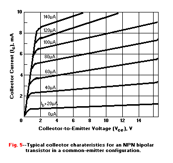
BJT can be better understood by examining the typical common-emitter
collector characteristics for a small-signal silicon NPN transistor
shown in Fig. 5. Direct current collector current Ic is
plotted on the Y axis, and DC collector-emitter voltage Vceo
is plotted along the X axis.
 A family of curves for different values of DC
base current Ib is drawn of Fig. 5. Base current is plotted
because the BJT is a current-operated device. As mentioned earlier, the
base-emitter junction is forward biased for normal transistor operation.
Base current flows and is a necessary variable for establishing the
BJT's operating point.
A family of curves for different values of DC
base current Ib is drawn of Fig. 5. Base current is plotted
because the BJT is a current-operated device. As mentioned earlier, the
base-emitter junction is forward biased for normal transistor operation.
Base current flows and is a necessary variable for establishing the
BJT's operating point.
 Observe the following specific points on Fig. 5:
When base current
(Ib is zero, the transistor conducts barely measurable
collector leakage current.
When the collector-to-emitter voltage
exceeds a few hundred millivolts, the collector current value is almost
directly proportional to the base current value. It is only slightly
affected by the actual collector voltage value. Thus, the transistor can
perform as a constant-current generator by feeding a fixed bias current
into the base.
The transistor can also perform as a linear
amplifier by superimposing the input signal on a nominal input bias
current. (This will be discussed in more detail later.)
Circuit
Applications:
Even a simple small-signal BJT has many
applications related to its ability to amplify or switch. Some of the
most important and practical circuit designs are described her. With few
exceptions, all of the circuits are based on the 2N3904 NPN transistor.
(With certain minor component value changes, other NPN transistor can be
substituted.) The circuits can also be made with a PNP transistor such
as the 2N3906, if the polarities are altered.
Diodes and Switches:
It was explained earlier that both the
base-emitter and base-collector junctions of a silicon BJT can be
considered equivalent to a zener diode. As a result, either of these
junctions can perform as a fast-acting rectifier diode or zener diode,
depending on the bias polarity.
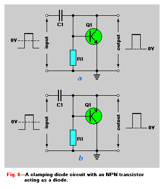
Figure 6 shows two alternative ways
to make an NPN BJT perform as a diode in a clamping circuit that
converts an AC-coupled rectangular input waveform into a DC square wave.
The input AC waveform is symmetrical above and below the zero-voltage
reference. However, the output signal retains the input's form and
amplitude, but it is clamped to the zero-voltage reference.
If you
build this circuit, use the base-collector terminals as the diode as in
Fig. 6-b because they provide a larger zener voltage value than the
circuit shown in Fig. 6-a.
Figure 7 shows how an NPN BJT can
function as a zener diode in a circuit that converts an  unregulated supply voltage into a fixed-value regulated
output voltage. Typical values range from 5 to 10 volts, depending on
the characteristics of the selected transistor. The base emitter
junction is the only one suitable for this application.
unregulated supply voltage into a fixed-value regulated
output voltage. Typical values range from 5 to 10 volts, depending on
the characteristics of the selected transistor. The base emitter
junction is the only one suitable for this application.
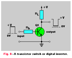
Figure 8
shows a BJT functioning as a simple electronics switch or digital
inverter. Here the base is driven through resistor Rb by a
digital input step voltage that has a positive value. The load resistor
Rl can be a simple resistor, tungsten lamp filament, or a
relay coil. Connect the load between the collector and the positive
supply.
When the input voltage is zero, the transistor switch is
cut off. Thus no current flows through the load, and the full supply
voltage is available between the collector and emitter terminals. When
the input voltage is high, the transistor switch is driven fully on.
Maximum current flows in the load, and only a few hundred millivolts is
developed between the collector and emitter terminals. Thus the output
voltage signal is the inverted form of the input signal.
 Linear
Amplifiers:
Linear
Amplifiers:
A BJT can function as a linear current or voltage
amplifier if a suitable bias current is fed into its base, and the
output signal is applied between a suitable pair of terminals. A
transistor amplifier can be configured for any of three operating modes:
common-emitter(Fig. 9), common-base(Fig. 10), and common-collector(Fig.
11). Each of these modes offers a unique set of characteristics.
In
the common-emitter circuit of Fig. 9, load resistor Rl is
connected between the collector and the positive supply, and a bias
current is fed into the base through Rb. The value of Rb
was selected so that the collector takes on a quiescent value of about
half the supply voltage (to provide maximum undistorted signal swings).
 The input signal in the form of a sine wave
is applied between the base and the emitter through C1. The circuit
inverts the phase of the input signal, which appears as an output
between the collector and emitter. This circuit is characterized by a
medium-value input impedance and a high overall voltage gain.
The input signal in the form of a sine wave
is applied between the base and the emitter through C1. The circuit
inverts the phase of the input signal, which appears as an output
between the collector and emitter. This circuit is characterized by a
medium-value input impedance and a high overall voltage gain.
The
input impedance of this amplifier is between 500 and 2000 ohms, and the
load impedance equals Rl. Voltage gain is the change in
collector voltage divided by the change in base voltage (from 100 to
about 1000). Current gain is the change in collector current divided by
the change in base current of Hfe.
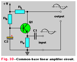
In the common-base
linear amplifier circuit of Figure 10, the base is biased through Rb
and AC-decoupled (or AC-grounded) through Cb. The input
signal is applied between the emitter and base through C1, and the
amplified but non-inverted output signal is taken from between the
collector and base. This amplifier offers very low input impedance, and
output impedance equal to the resistor Rl. Voltage gain is
from 100 to 1000, but current gain is near-unity.

 In the common-collector linear amplifier circuit of Fig.
11, the collector is connected directly to the positive voltage supply,
placing it effectively at ground impedance level The input signal is
applied directly between the base and ground (collector), and the
non-inverted output signal is taken between the emitter and ground
(collector).
In the common-collector linear amplifier circuit of Fig.
11, the collector is connected directly to the positive voltage supply,
placing it effectively at ground impedance level The input signal is
applied directly between the base and ground (collector), and the
non-inverted output signal is taken between the emitter and ground
(collector).
The input impedance of this amplifier is very high; it
is equal to the product of hfe and the load resistance Rl.
However, output impedance is very low. The circuit's overall voltage
gain is near-unity, and its output voltage is about 600 millivolts less
than the input voltage. As a result, this circuit is know as a
DC-voltage follower or an emitter follower. A circuit with very high
input impedance can be obtained by replacing the single transistor of
the amplifier of Fig. 11 with a pair of transistors connected in a
Darlington configuration, as shown in Fig. 12. Here, the emitter current
of the input transistor feeds directly into the base of the output
transistor with an overall hfe value equal to the product of
the values for the individual BJT's. 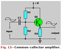 For
example, if each BJT has an hfe of 100, the pair acts like
single transistor with an hfe of 10,000. Darlington BJT's
with two transistors on a single chip (considered to be discrete device)
are readily available for power amplification.
For
example, if each BJT has an hfe of 100, the pair acts like
single transistor with an hfe of 10,000. Darlington BJT's
with two transistors on a single chip (considered to be discrete device)
are readily available for power amplification.
The voltage-follower
circuit of Fig. 11 can be modified for an alternating current input by
biasing the transistor base with a value equal to half the supply
voltage and feeding the input signal to the base. Figure 14 shows how
this particular circuit is structured.
The emitter-follower
circuits of Figs. 12 to 14 can source or feed relatively high currents
into an external load through the emitter of the transistor. However,
those circuits cannot sink or absorb high currents that are fed to the
emitter from an external voltage source because the emitter is
reverse-biased under this condition. As a result, these circuits have
only a unilateral output capability.
In many applications, (such as
audio amplifier output stages), a bilateral output characteristic is
essential. A bilateral amplifier has equal sink and source output
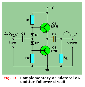
capabilities. This is obtained with the complementary emitter-follower
circuit of Fig. 14. The series-connected NPN-PNP transistor pair is
biased to give a modest quiescent current through the network consisting
of resistors R1 and R2 and diodes D1 and D2. Transistor Q1 can provided
large source currents, and Q2 can absorb large sink currents.

Phase Splitters:
Transistor linear amplifiers can be used in
active filters or oscillators by connecting suitable feedback networks
between their inputs and outputs. Phase splitting is another useful
linear amplifier application. It provides a pair of output signals from
a single input signal: one is in phase with the input phase, and the
other is inverted or 180° out of phase. Fig. 16 and 17 show these
alternative circuits.
In the circuit shown in Fig. 15, the BJT is
connected as a common-emitter amplifier with nearly 100% negative
feedback applied through emitter resistor R4. It has the same value as
collector resistor R3. This configuration provides a unity-gain inverted
waveform at output 1 and a unity-gain non-inverted waveform at output 2.
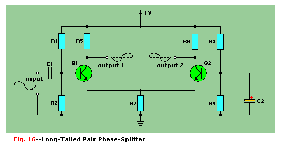
The phase-splitter circuit shown in Fig. 16 is known as a long-tailed
pair because the two BJT's share common-emitter feedback resistor R7. An
increasing waveform applied at the base of transistor Q1 causes the
voltage to increase across resistor R7, reducing the bias voltage on
transistor Q2. This results in the generation of an inverted waveform at
the collector of Q1 (at output 1), and an in-phase waveform at the
collector of Q2, (at output 2).

 Multivibrators:
Figures 17 to 20 show BJT's in the four
different kinds of multivibrator circuit: bistable, astable, monostable,
and Schmitt trigger.
The bistable multivibrator is a simple
electronic circuit that has two stable states. It is more often known as
the flip-flop, but is also called a binary multivibrator, or an
Eccles-Jordan circuit. The circuit is switched from one state to the
other by a pulse or other external signal. It maintains its state to the
other by a pulse or other external signal. It maintains its state
indefinitely unless another input signal is received.
Figure 17 is
a simple, manually-triggered, cross-coupled bistable multivibrator. The
base bias of each transistor is obtained from the collector of the other
transistor. Thus one transistor automatically turns OFF when the other
turns ON, and this cycle can be continued in definitely as long as it is
powered.
The output of the multivibrator in Fig. 17 can be driven
low by turning off transistor Q2 with switch S2. The circuit remains
'locked' or stable in this state until transistor Q1 is turned off with
switch S1. At that time, the output is locked into its high state, and
the process is repeated. It can be seen that this action makes it a
simple digital memory circuit that holds its state until manually or
electronically switched.
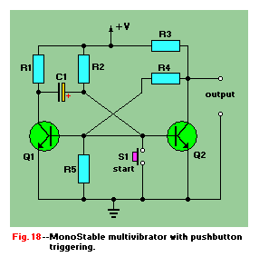
Figure 18 is the schematic for a
monostable multivibrator or one-shot pulse generator. It has only one
state. The output of this circuit, a manually triggered version, is
normally low, but it switches high for a period determined by the values
of capacitor C1 and resistor R2 if transistor Q1 is turned off with
switch S1. It then returns to tits original state.
The pulse
duration time of the monostable multivibrator can be determined from the
equation: colr = '#0000ff'>T = 0.69 RC
Where: T is in
microseconds, R is in ohms, and C is in microfarads.
Monostable
multivibrators are used as pulse generators and weep generators for
cathode-ray tubes.
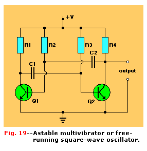
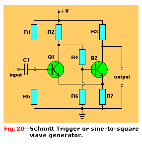 Figure 19 is the schematic for an astable multivibrator
or free-running, square-wave oscillator. The transistors are in a
common-emitter configuration so that the output of one is fed directly
to the input of the other. Two resistance-capacitor networks, R3 and C1,
and R2 and C2, determine the oscillation frequency.
Figure 19 is the schematic for an astable multivibrator
or free-running, square-wave oscillator. The transistors are in a
common-emitter configuration so that the output of one is fed directly
to the input of the other. Two resistance-capacitor networks, R3 and C1,
and R2 and C2, determine the oscillation frequency.
The output of
each transistor is 180° out of phase with the input. An oscillating
pulse might begin at the base of Q1. It is inverted at the collector of
Q1 and is sent to the base of Q2. It is again inverted at the collector
of Q2 and therefore returns to the base of Q1 in its original phase.
This produces positive feedback, resulting in sustained oscillation.
The astable multivibrator is frequently used as an audio oscillator, but
is not usually used in radio-frequency circuits because its output is
rich in harmonics.
Figure 20 is a schematic for a Schmitt Trigger,
a form of bistable multivibrator circuit. It produces rectangular waves,
regardless of the input waveform. The circuit is widely used to convert
sine waves to square waves where these is a requirement for a train of
pulses with constant amplitude.
The Schmitt trigger circuit remains
off until the rising input waveform crosses the preset threshold
trigger-voltage level set by the value of resistors R1 and R2. When
transistor Q1 is switched 'on', transistor Q2 is 'off' and, the Schmitt
trigger's output voltage rises abruptly.
When the input signal
falls back below its drop-out level, Q1 switches 'off' and Q2 switches
'on'. The output voltage of the Schmitt trigger drops to zero almost
instantly. This cycle of events will then be repeated in definitely, as
long as the input signal is applied.